- Business
-
SiC
-
SiC
-
SiC
-
SiC

SiC(Semiconductor materials)
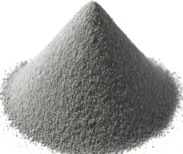
SiC High-Purity Powder Manufacturing Technology and Related Organic/Inorganic Raw Material Synthesis
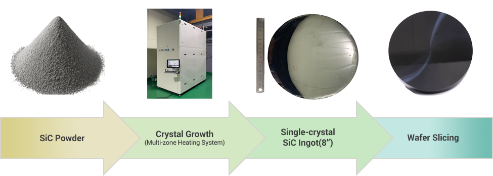
This technology enables the production of SiC powders with a purity of 99.9999% or higher, serving as the starting material for SiC ingot growth. Through processes such as synthesizing organosilicon compounds with partners like Company S and thermally decomposing them, or reacting high-purity silica with carbon-based materials to obtain SiC powders, UNIS has established an independent supply chain for high-quality raw materials.
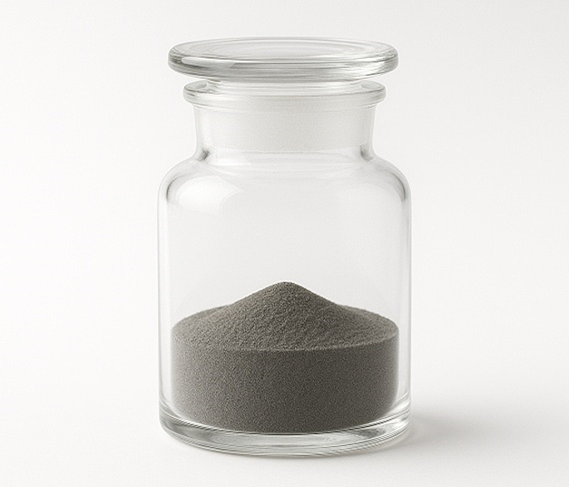
High-Purity SiC Powder
Product Description
Developed using advanced inorganic and organic synthesis technologies, this powder is designed for high-performance semiconductor and display manufacturing processes.
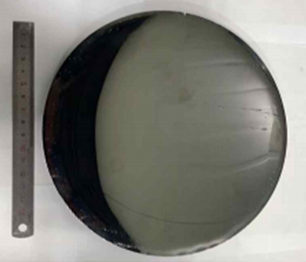
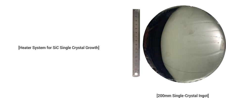
8-inch SiC Single Crystal Ingot
Product Description
Fabricated using advanced multi-zone resistance heating systems and precision slicing technologies, this ingot demonstrates our capability in large-diameter SiC wafer production.
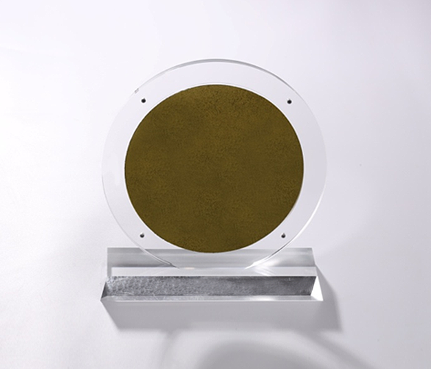
8-inch SiC Wafer for Power Devices in Electric Vehicles
Product Description
Designed for high-efficiency power conversion, this conductive SiC wafer supports next-generation electric vehicle inverters and fast-charging systems, enabling higher power density and improved thermal performance compared to conventional silicon wafers.
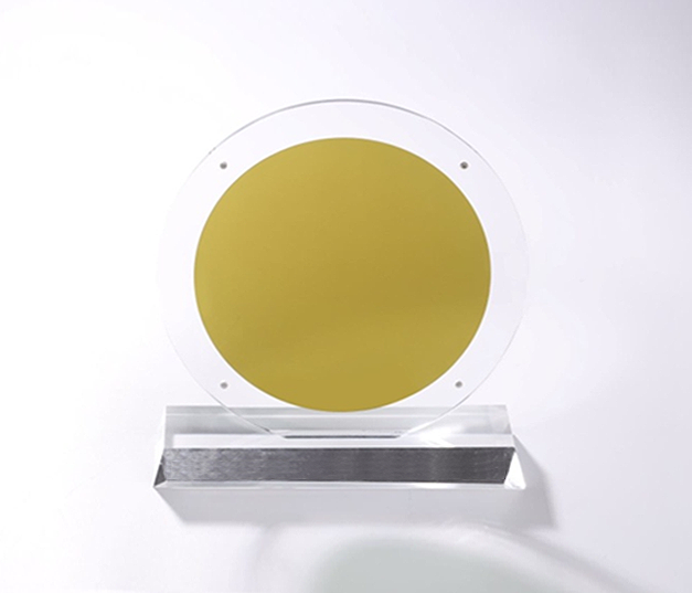
8-inch Semi-Insulating SiC Wafer for Communication
Product Description
This wafer is designed for high-frequency, high-power RF and microwave communication systems, offering exceptional thermal conductivity and low signal loss. With an 8-inch diameter, it enables larger-scale device fabrication, improving manufacturing efficiency and yield. The semi-insulating property ensures minimal electrical leakage, making it ideal for 5G base stations, satellite communication, radar systems, and advanced wireless infrastructure. This exhibit highlights UNIS’s capability to produce large-diameter, high-quality semi-insulating SiC wafers to meet the demands of next-generation communication technologies.
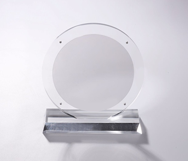
8-inch SiC Wafer for AR Lenses
Product Description
This wafer is engineered for use in advanced Augmented Reality (AR) optical systems, delivering exceptional optical transparency, mechanical strength, and thermal stability. The 8-inch diameter enables large-scale lens substrate production, improving manufacturing efficiency for AR devices. SiC’s high refractive index and durability make it ideal for thin, lightweight AR lenses that must endure high-intensity projection light and environmental stress. This exhibit showcases UNIS’s capability to produce high-purity, defect-controlled SiC wafers optimized for precision optics in next-generation AR glasses and headsets.
UNIS’s 200mm SiC Ingot & Wafer (for Power Semiconductors) – Features & Advantages
Enhanced Productivity through Larger Wafer Size
The 8-inch (200 mm) wafer offers approximately 78% larger active area compared to the 6-inch wafer, enabling higher chip yields per wafer. This leads to lower cost per chip and improved efficiency in mass production.
Superior Crystal Quality
Characterized by an ultra-low micropipe density (≤ 0–10 cm⁻²), ensuring uniform electrical properties across the wafer. The precise crystal orientation (<0001> ± 0.5°) enhances device performance and process consistency.
Outstanding Electrical Performance
Flexible n-type and p-type doping options tailored to diverse device requirements such as MOSFETs, SBDs, and IGBTs. With a low-resistivity range (n-type: 0.015 ~ 0.030 Ω·cm), the wafer supports higher current handling and minimizes conduction losses.
Precision Surface Processing
Optimized for advanced lithography and epitaxy, featuring CMP-polished surface (frontside Ra ≤ 0.2 nm). Maintains excellent thin-film uniformity with low Total Thickness Variation (TTV ≤ 10 µm).
Excellent Thermal & Mechanical Properties
High thermal conductivity enables efficient heat dissipation and supports high-power device design. A wide bandgap (3.26 eV) ensures reliable high-voltage operation with reduced switching losses. Stable mechanical strength is maintained even in ultra-thin wafer formats.
Advanced Manufacturing Technologies
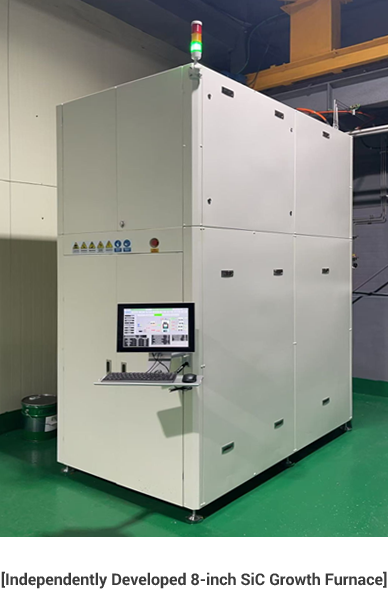
Equipped with thermodynamic heater design and multi-zone control to stabilize large-diameter crystal growth. Laser slicing technology minimizes material loss and improves yield compared to conventional diamond wire cutting. Capability to produce bonded wafers, supporting a variety of next-generation high-performance device structures.
| ITEM | 6-inch | 8-inch | Remarks |
|---|---|---|---|
| Diameter | 1500mm | 2000mm | Approx. 33% increase |
| Area | ~17,671㎟ | ~31,416㎟ | Approx. 78% increase |
| Number of wafers per ingot | Standard | ~1.78× | Factors such as slicing loss need to be considered |
| Number of chips per wafer (based on 5 mm) | ~260 | ~460 | Approx. 77% increase |
| Unit cost per chip | Higher | Lower (improved efficiency per area) | Productivity improvement |
| Equipment production efficiency | Reduced | High | Increased output per equipment unit |
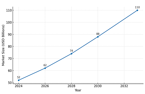
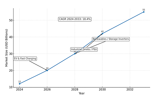
Global Power Semiconductor Market Outlook (lllustrative)
The global power semiconductor market is projected to grow from approximately USD 52 billion in 2024 to USD 110 billion by 2034.Over the next decade, the industry is expected to maintain a strong and steady growth trajectory, clearly highlighting the immense potential and future opportunities of the power semiconductor sector.